Nanoanalytics Center - Advanced Microscopy

Group Leader Center for Nanoanalytics

Bridge Professor Center for Nanoanalytics
Exploring the smallest structures, penetrating the world of atoms.
The Nanoanalytics Center is a renowned facility that is intensively involved in the research and analysis of the smallest structures, providing a fascinating insight into the world of atoms. As a leading research and service center, we have extensive expertise, state-of-the-art analytical equipment and innovative methods that are specifically focused on the development of materials, materials and products.
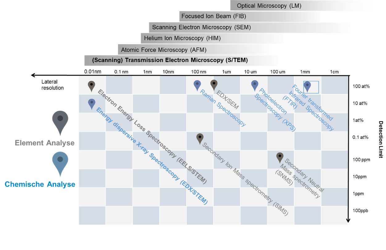
Using this outstanding equipment, we are able to precisely determine atomic and chemical composition, covering a wide range of length scales - from centimeters to the atomic scale.
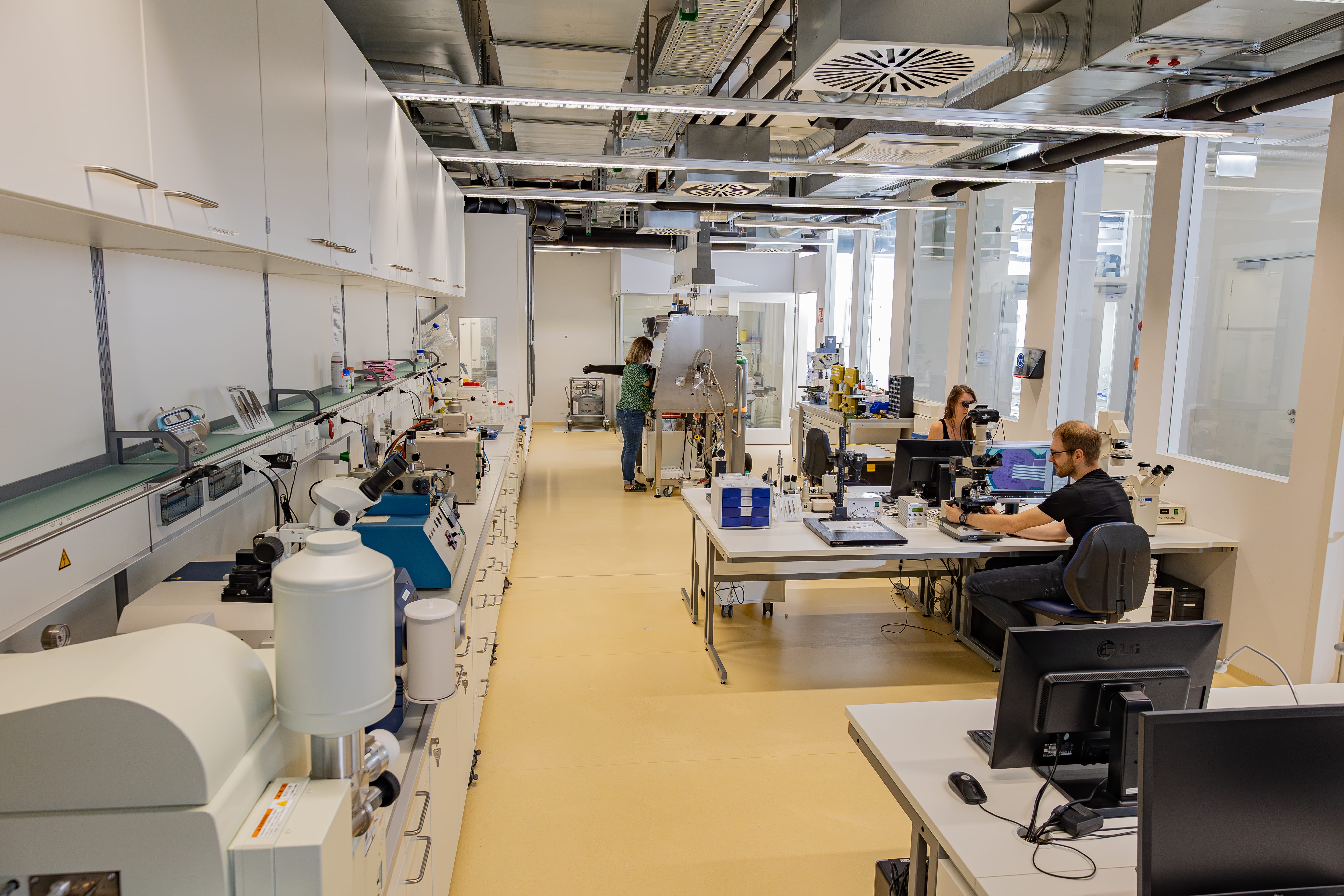
The Nanoanalytics Center is staffed by a highly qualified team of mostly PhD scientists and engineers with specialties in physics, chemistry, materials science, mineralogy and environmental engineering. Working closely together, we solve complex problems for demanding customers from industry and research. Our expertise and passion drive the discovery of innovative solutions.
Our goal is to continuously push the boundaries of knowledge and technological possibilities in the field of nanoanalytics and to provide our customers from industry and research with a decisive competitive edge.
The team of the Nanoanalytics Center sees itself as a link between science and industry. Our range of services includes analytical services, consulting and technology assessment.
Our Expertise
Non-falsifying sample preparation
Our highly experienced team has over 30 years of expertise in non-falsifying sample preparation for precise analysis of material surfaces, medical instruments and components. In addition, we offer a full chain for processing aqueous or non-vacuum samples under cryogenic conditions. Here, we can analyze samples in an optical microscope with a cryo stage and then further investigate them with a special shuttle in cryo FIB-SEM. Our expertise, equipment and experience make us your reliable partner.
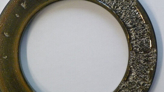
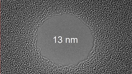
Interfacial, microstructure and nanoparticle analytics.
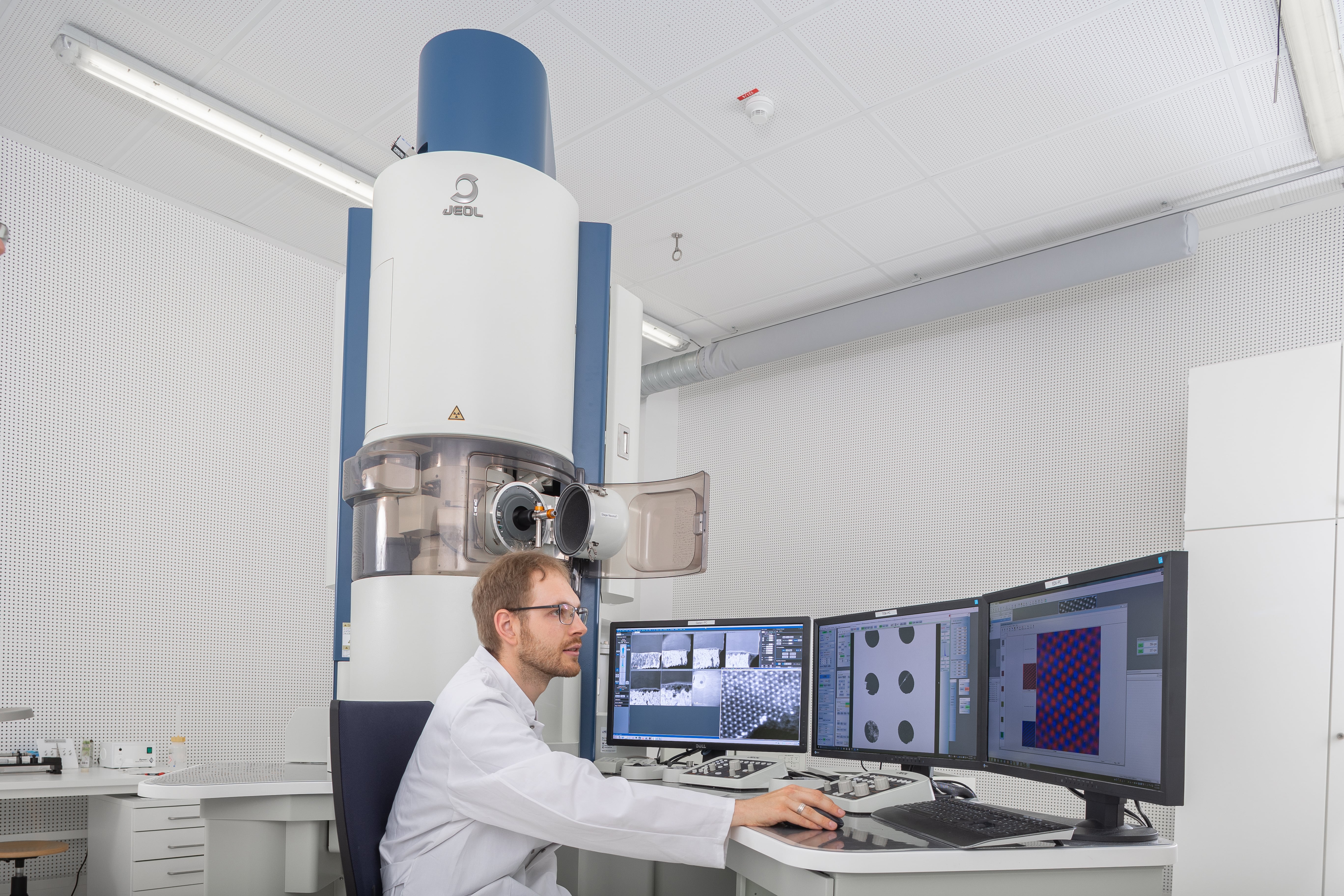
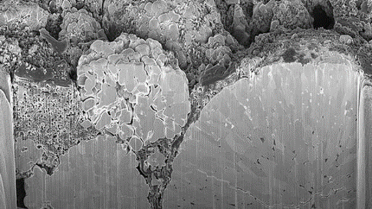
Surface analytics systems are critical to the study of surfaces. AFM, SEM, XPS, and surface profilometers can detect defects, investigate structure-property relationships, and make precise measurements. SEM reveals surface structures, EDX determines chemical composition. EELS in TEM provides atomic information about bonds. ToF-SIMS in a FIB-SEM enables sensitive detection of elements such as lithium for battery research.
These techniques are essential for materials development, quality control, and surface modification in a variety of fields. Precise analysis and imaging of processes and effects on material surfaces plays a major role in the optimization of medical instruments, components in mechanical and automotive engineering, and other interfaces with high spatial resolution.
Our Analytics at a Glance
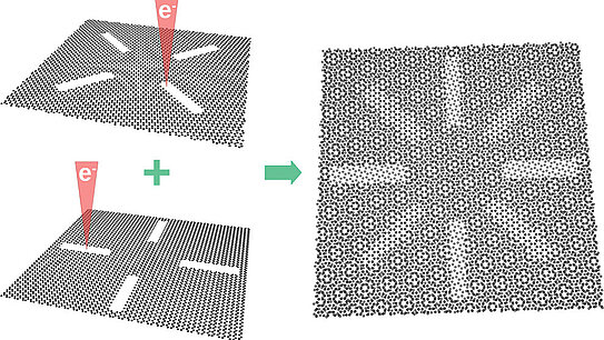
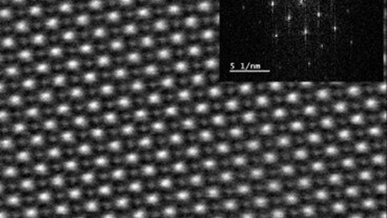
Advanced materials analysis techniques are applied to a wide range of functional materials and devices to understand and improve their microstructure-property correlation. Our cutting-edge equipment includes two high-resolution analytical electron microscopes, which we use for materials research and investigation to elucidate the atomic structure of crystal defects, interfaces, and surface layers, leading to a deeper understanding of the material properties that occur.
Exemplary is mentioned here:
Nanoanalytics for functional materials and thin film systems in electronics, sensor technology and surface engineering or the investigation of nanostructures, layer thicknesses, interfaces and defects in solids and materials.
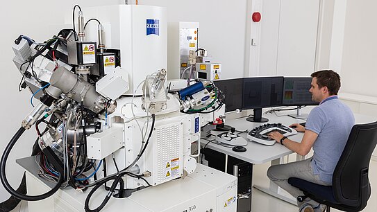
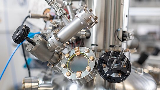
Our Equipment
Services offered by the Nanoanalytics Center
Analysis of Energy and Battery Materials

Research topics at the Nanoanalytics Center
Funded by
NMI Natural and Medical Sciences Institute
at the University of Tübingen
Markwiesenstraße 55, 72770 Reutlingen
Tel.: +49 7121 51530-0
Mail: info@nmi.de
Follow us now