Research on low-dimensional materials

Material-, Interfacial and Nanoanalytics
Bridge Professor
Senior Principal Scientist
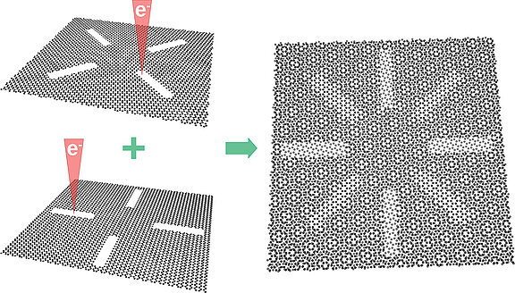
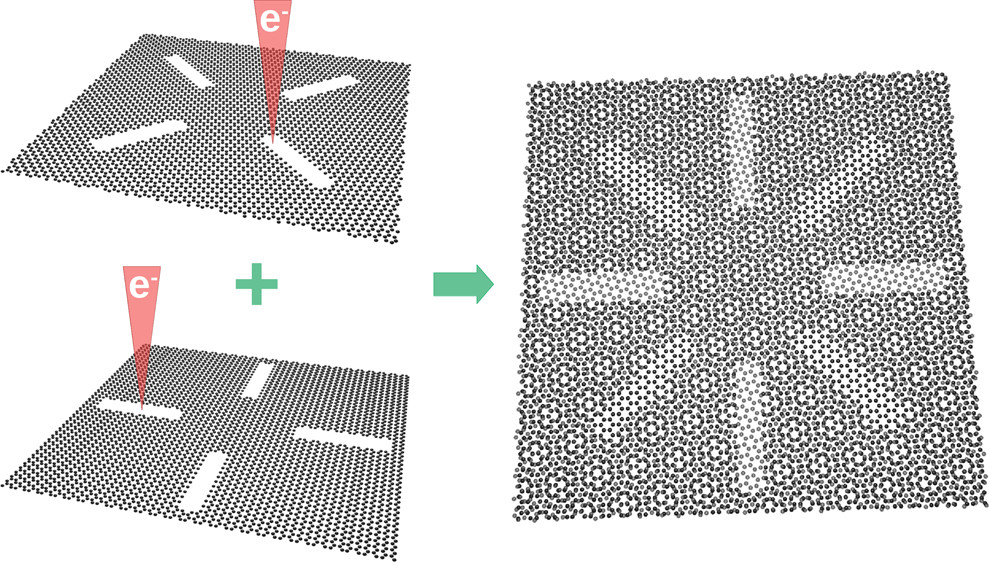
Nanostructuring and stacking of 2D materials are combined to create novel 3D structures.
Two-dimensional materials can be stacked in any order. Since each plane is only one or a few atoms thick, stacking results in control over the material structure along one dimension with near atomic resolution. In addition, isolated, cantilevered 2D materials can be patterned with very high resolution using focused electron or ion beams. We combine the capabilities of patterning 2D materials using focused electron and ion beams with the composition of single atomic layers in heterostructures. If this can be achieved with high accuracy of fit, novel 3D structures with nanometer resolution can be generated in this way. In addition, other materials, such as molecular layers or reactive metals, are also embedded between 2D materials. By confinement in 2D materials, we can investigate structures in the electron microscope that are not compatible with conventional sample carriers.
Functionalization
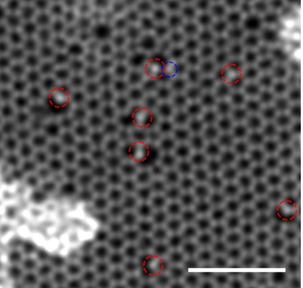
In low-dimensional materials such as carbon nanotubes, graphene, or other 2D materials, virtually all of the atoms are on the surface and are thus accessible to adsorption and desorption of gases from the outside. The porosity and surface-to-volume ratio in these materials can therefore be extremely large. However, since the surfaces of these materials are usually very inert, functional groups must be inserted to exploit these properties. Using low energy ion irradiation, we introduce defects into the materials or insert foreign atoms into the structure as dopants. These structural modifications are verified by atomic-resolution electron microscopy and optimized iteratively.
Atomically Resolved Analysis
Aberration-corrected transmission electron microscopy or scanning transmission electron microscopy can in principle be used to resolve all atomic distances. Atomically resolved electron microscopy, however, should ideally provide not only the position of individual atoms, but also their chemical identity. For this purpose, spectroscopic analysis is usually used, in which only a single atom or column of atoms is excited by the electron beam. However, this is particularly challenging for low-dimensional materials due to the low stability of the sample under the electron beam, as they often do not hold still long enough to perform a full atomic-resolution spectroscopic analysis. Here, we additionally use the information contained in the scattering intensity - simply put, the fact that heavier atoms in the image also have a higher contrast - to analyze complex 2D structures. For this purpose, image simulations are automatically adjusted until not only the shape of the atoms but also the contrast matches the experimental data.
NMI Natural and Medical Sciences Institute
at the University of Tübingen
Markwiesenstraße 55, 72770 Reutlingen
Tel.: +49 7121 51530-0
Mail:
info@nmi.de
Follow us now