Parylene coating

Group Leader Biomedical Micro and Nano Engineering
Parylene is an ideal choice for coating and protecting devices for a wide range of applications, from electronics and semiconductors to medical devices and aerospace components.
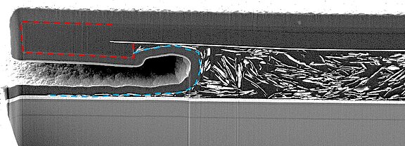
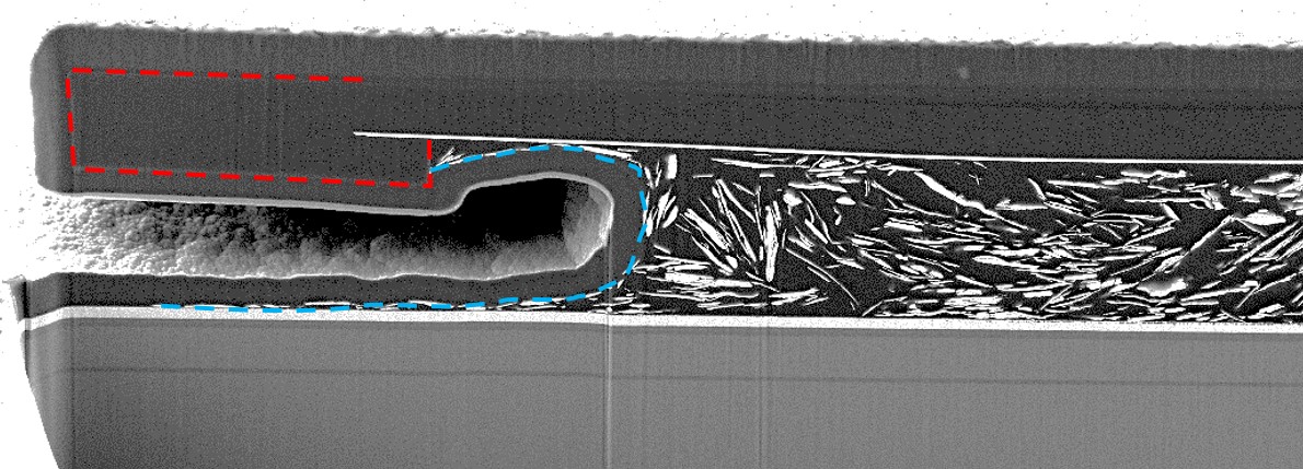
The deposition of parylene is unique: it is deposited via a vapor-phase process, resulting in ultra-thin, pinhole-free coatings. Parylene coats conformally even on high-aspect-ratio features and buried structures. Deposition at room temperature makes it suitable for most materials. Parylene’s exceptional characteristics include excellent chemical and solvent resistance, superior dielectric strength, and a low coefficient of friction.
Our parylene coating services are designed to support research, development, and production across various industries. A common recipe consists of pretreatment by oxygen plasma, functionalization by an A174 adhesion promoter and coating with several micrometers of parylene C. We also offer variations in adhesion promoters and other forms of parylene (parylene F, parylene D, etc.).
Our services extend beyond standard coatings to include biological evaluation, material functionalization and advanced material and surface analysis.
Applications across industries:
- Electronics and PCBs: Enhance the reliability of your devices with coatings that protect against moisture and chemical damage.
- Medical Devices: Ensure the safety and longevity of implants and surgical tools with biocompatible parylene coatings.
- Aerospace and Automotive: Equip your components with protection against extreme environmental conditions.
- Sensors and Optics: Preserve the accuracy of your instruments by shielding sensitive surfaces from contaminants.
For further information or to discuss your specific parylene coating needs, please contact us. Whether you're in the research phase or scaling up production, our team is here to provide expert advice and custom solutions tailored to your specific needs.
NMI Natural and Medical Sciences Institute
at the University of Tübingen
Markwiesenstraße 55, 72770 Reutlingen
Tel.: +49 7121 51530-0
Mail: info@nmi.de
Follow us now