New Ways to Nanostructure and Stack 2D Materials

Group Leader Advanced Materials
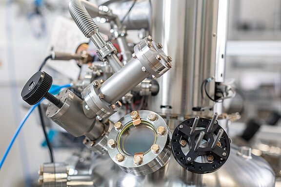
Atomically resolved analysis and manipulation of 2D materials.
Two-dimensional materials can be stacked on top of each other in any desired way. In this way, what are known as "van der Waals heterostructures" due to their underlying bonding, can be produced in a targeted manner. Since each plane is only one or a few atoms thick, stacking gives control over the material structure along a dimension material structure along one dimension with nearly atomic resolution. In addition, isolated, cantilevered 2D materials can be can be patterned with very high resolution using focused electron orion radiation.
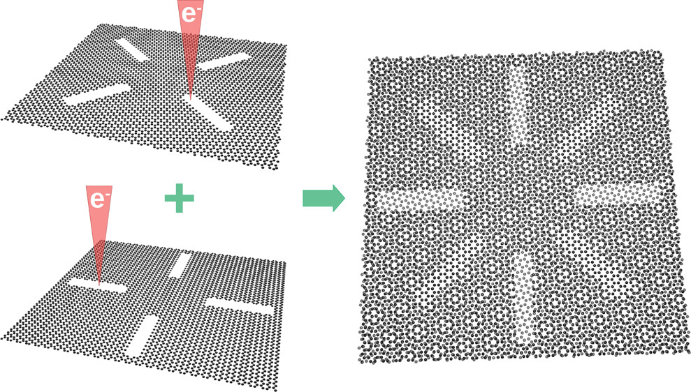
Control over the morphology within each plane of a van der Waals heterostructure has been very limited. In this project, we will explore a fundamentally new way to fabricate almost any 3D structure. To do this, we will combine the capabilities of patterning 2D materials using focused electron and ion beams with the composition of individual atomic layers in heterostructures. With a definition of structures in each plane prior to targeted stacking, it should be possible to create arbitrary 3D structures. This is similar to the concept of 3D printing, except that the individual layers can be as thin as one atom and patterning in each plane should likely be possible with sub-nanometer resolution.
In connection with the structuring, we will also investigate in particular how the properties of the materials can be specifically changed by nanostructuring and also in combination with the interaction between the layers. To this end, we will study the resulting structures using transmission electron microscopy, Raman spectroscopy and other optical methods, as well as transport measurements. The experimental results will be analyzed using detailed simulations. The simulations will also help to find optimal parameters for nanostructuring and for influencing the properties. Overall, the project will enable new material structures, new possibilities for the targeted manipulation of material properties, and new ways to fabricate nanostructured devices.
Research content
- Structuring of 2D materials by scanning transmission electron microscopy
- Structuring of 2D materials using focused ion beams
- Structuring of 2D materials by electron beam induced etching
- Stacking of nanostructured 2D materials
- Modification of properties by nanostructuring and stacking
NMI Natural and Medical Sciences Institute
at the University of Tübingen
Markwiesenstraße 55, 72770 Reutlingen
Tel.: +49 7121 51530-0
Mail: info@nmi.de
Follow us now