Microfabrication

Group Leader Biomedical Micro and Nano Engineering
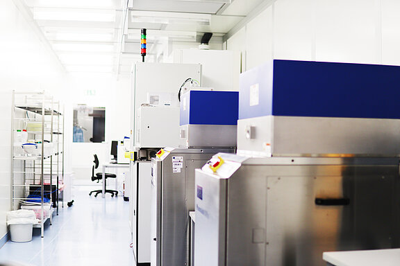
Microfabrication is a precision-driven technique for creating detailed structures and devices at the micrometer scale. While its roots are in semiconductor manufacturing, its applications have expanded into diverse fields such as biomedical and microfluidics.
This method allows the creation and modification of structures with remarkable precision, even down to several nanometers in special cases. Our team of experts can provide individual process steps or develop comprehensive workflows tailored to your specific needs.
Core Offerings:
Plasma Enhanced Chemical Vapor Deposition (PECVD): Leverage the benefits of plasma to increase deposition rates and ensure substrate uniformity and superior film quality, even at ambient temperatures.
PVD (Physical Vapor Deposition): Achieve superior thin film coatings with our state-of-the-art PVD techniques, known for optimal adhesion and elemental purity.
Chemical Vapor Deposition (CVD): Use our CVD processes to deposit high-quality, uniform, defect-free films suitable for a wide range of applications.
Spin Coating: Our spin-coating capabilities enable unsurpassed results across a spectrum of polymers, ensuring precision in uniformity and thickness control.
Dry Etching: Our advanced dry etching solutions provide anisotropic etch profiles critical for detailed micro- and nanostructures.
Reactive Ion Etching (RIE): Leverage our RIE capabilities for unmatched etch rates, selectivity, and precise pattern transfer, making them essential for precision microfabrication programs.
Wet Etching: Our wet etching services provide an isotropic material removal method optimal for bulk etching and specific pattern transfer.
Electroplating: Delve into our specialized electroplating services focused on creating intricate 3D structures. Our techniques ensure metal structures with defined shapes, improved adhesion, and uniform thickness.
Characterization: Beyond fabrication, our detailed characterization services provide comprehensive insight into the thicknesses of your manufactured layers. Using SEM imaging, we provide tangible confirmation of the success and accuracy of our manufacturing protocols.
Why partner with us?
With a team of experienced professionals and a repertoire of advanced tools, we are uniquely positioned to meet the diverse needs of microfabrication. We back every offering with rigorous quality assurance and an unwavering commitment to precision.
Whether your interests span research, development, or large-scale industrial production, we're well-equipped and eager to support your microfabrication goals. Let's build the future together, one micron at a time.
Contact us today and discover how our offerings can make a difference in your endeavors.
Standard processes:
- PVD Sputtering - Au, Ti, Cr, ITO, TiN
- Electroplating – Au, Ag, Ni
- PECVD – SiN, SiO2
- CVD – Parylene C
- RIE – CF4, O2, CHF3
- Dry etching - Ar
- Spincoating – Polyamide, SU-8
- Wirebonding – Au
Characterization:
- Impedance spectroscopy
- 4 point resistivity
- Laser scanning microscope (Keyence)
- Scanning Electron Microscope / Focused Ion Beam/ EDX
- Profilometry
NMI Natural and Medical Sciences Institute
at the University of Tübingen
Markwiesenstraße 55, 72770 Reutlingen
Tel.: +49 7121 51530-0
Mail: info@nmi.de
Follow us now